SN74AVC1T45DBVR Features
* Available in the Texas Instruments NanoFree rwPackage
* Fully Configurable Dual-Rail Design Allows EachPort to Operate Over the Full 1.2-V to 3.6-VPower-Supply Range
* Vcc lsolation Feature lf Either Vcc Input ls AtGND, Both Ports Are In The High-lmpedance State
* DIR Input Circuit Referenced to VccA+12-mA Output Drive at 3.3 V
* I/Os Are 4.6-V Tolerant
* loff Supports Partial-Power-Down Mode Operation
* Typical Max Data Rates
- 500 Mbps (1.8-V to 3.3-V Translation)
- 320 Mbps (<1.8-V to 3.3-V Translation)
- 320 Mbps (Translate to 2.5 V or 1.8 V)
- 280 Mbps (Translate to 1.5 V)
- 240 Mbps (Translate to 1.2 V)Latch-Up Performance Exceeds 100 mA PerJESD 78, Class ll
* ESD Protection Exceeds JESD 22
- ±2000-V Human Body Model (A114-A)
- 200-V Machine Model (A115-A)
- ±1000-V Charged-Device Model (C101)
SN74AVC1T45DBVR Applications
• Personal Electronic
• Industrial
• Enterprise
• Telecom
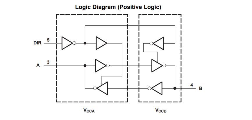
SN74AVC1T45DBVR Description
This single bit noninverting bus transceiver uses twoseparate configurable power-supplyrails.TheSN74AVC1T45 is optimized to operatewithVcca/VccB set at 1.4 V to 3.6 V. It is operational withVcca/Vccs as low as 1.2 V. The A port is designed totrack Vcca. Vcca accepts any supply voltage from 1.2V to 3.6 V. The B port is designed to track VccB. VccBaccepts any supply voltage from 1.2 V to 3.6 V. Thisallowsfor universallow voltage,bidirectionatranslation between any of the 1.2-V15 V,1.8-V.2.5-V, and 3.3-V voltage nodes.