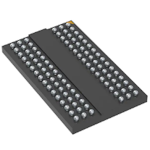
AS4C128M16D3C-93BCNTR
128M x 16 bit DDR3 Synchronous DRAM (SDRAM)
Overview
The 2Gb Double-Data-Rate-3 DRAMs is double data rate architecture to achieve high-speed operation. It is internally configured as an eight bank DRAM. The 2Gb chip is organized as 16Mbit x 16I/Os x 8 bank devices. These synchronous devices achieve high speed double-data-rate transfer rates of up to 2133 Mb/sec/pin for general applications. The chip is designed to comply with all key DDR3 DRAM key features and all of the control and address inputs are synchronized with a pair of externally supplied differential clocks. Inputs are latched at the cross point of differential clocks (CK rising and CK# falling). All I/Os are synchronized with differential DQS pair in a source synchronous fashion.
Features
JEDEC Standard Compliant
Power supplies: VDD & VDDQ = +1.5V ± 0.075V
Operating temperature range: (Commercial)
- Normal Operating temperature: TC = 0~85°C
- Extended temperature: TC = 85~95°C
Supports JEDEC clock jitter specification
Fully synchronous operation
Fast clock rate: 1066MHz
Differential Clock, CK & CK#
Bidirectional differential data strobe
- DQS & DQS#
8 internal banks for concurrent operation
8n-bit prefetch architecture
Pipelined internal architecture
Precharge & active power down
Programmable Mode & Extended Mode registers
Additive Latency (AL): 0, CL-1, CL-2
Programmable Burst lengths: 4, 8
Burst type: Sequential / Interleave
Output Driver Impedance Control
Average refresh period
- 8192 cycles/64ms (7.8us at 0°C ≦ TC ≦ +85°C)
- 8192 cycles/32ms (3.9us at +85°C ≦ TC ≦ +95°C)
Write Leveling
ZQ Calibration
Dynamic ODT (Rtt_Nom & Rtt_WR)
RoHS compliant
Auto Refresh and Self Refresh
Package: Pb and Halogen Free
- 96-ball 7.5 x 13 x 1.0mm FBGA


